

Chip components 0201 and 0402 weigh only a few thousandths of a gram, and the amount of tin used to make the solder joints for them is also very small. At that scale, a difference of a few tens of micrometers in the amount of solder paste is enough to turn a successful solder joint into a defect — but it is very difficult to detect with the naked eye or with conventional optical inspection.
This article guides you on reading solder cross-sections of small chip components, identifying three main defects: tombstone, insufficient solder and solder bridge, as well as design factors that affect the results.
1. Why are small chip components difficult to test?
- Tin volume is too small: The absolute error is small but the error ratio over the total amount of tin is large.
- The solder joint is located under the two ends of the component: Most of the link area is hidden.
- Optical inspection is difficult to expand the viewing angle: The components are low, the bottom part of the foot cannot be seen.
- Easily affected by manipulation: The suction force of the pick-up head and slight collision will also cause movement.
2. Four characteristics to read on a cross-section
| Characteristics | Normal signs | Signs to pay attention to |
|---|---|---|
| Fillet at both ends | The tin rises evenly at both ends, with a smooth concave shape | One end has tin, the other has almost none |
| Contact width | Tin is coated evenly across the width of the component head | The tin is tilted to one side, unevenly |
| Gap under foot | There is no gap between the foot and the pad | There are gaps, especially after bending or mechanical impact |
| Void in the solder joint | None or very small | Large voids occupy a significant portion of the solder joint |
3. Three main defects and signs on the section
| Error | Marks on the cross-section | Common causes |
|---|---|---|
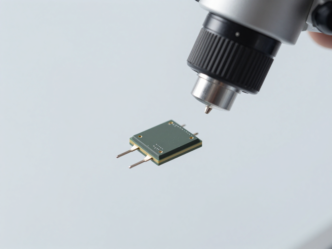
| Tombstone (lift one end) | One end of the component is up, with a gap under the other end | Imbalance of surface tension between the two ends |
| Tin deficiency | Fillet is thin, tin does not climb to the top of the component | The amount of solder paste is not enough, the stencil opening is small, the solder paste is dry |
| Tin bridge | Tin connects two adjacent electrodes or pads | Excess amount of solder paste, small pad gap, component pressure |
| Large void underfoot | Air bubbles occupy most of the solder joint area | The solder paste is damp and the gas cannot escape in time during the melting process |
Point to emphasize: tombstone is not a component error but an imbalance error during the solder jointing process. The cross-section helps confirm the clearance under the component head, which is direct evidence of this type of defect.
4. Why does tombstone happen?
When the solder paste melts, surface tension forces pull the component toward the melting mass of tin. If the two ends do not melt at the same time, the pulling force is unbalanced and one end lifts up. Common causes:
- Heat difference between two ends: due to uneven copper density around the pad or due to the direction of the heat exchanger.
- Difference in solder paste amount: one end has more cream due to stencil or misprinting.
- Asymmetrical pad: a larger pad or connected to a large copper area.
- One end is oxidized: Tin is impervious to wetting on one side.
- Vibration or impact when the tin is still molten.
5. Influence of design and stencil
| Factor | Influence | How to control |
|---|---|---|
| Stencil thickness | Decide on the amount of solder paste for each pad | Choose the thickness according to the size of the smallest component on the board |
| Stencil open area | Affects the amount of cream and fillet shape | Use the appropriate opening ratio, avoid opening too large |
| Pad spacing | Decide the risk of solder bridges | Check according to component design recommendations |
| Copper area around the pad | Create a heat difference between the two ends | Thermal symmetry design between two pads |
| Location of components | Affects tension when tin melts | Control component placement tolerances |
6. Additional testing should be combined
- Measuring shear force (shear test) on the solder joint to evaluate the bond strength.
- Try heat shock to evaluate the ability of small solder joint joints to withstand thermal cycling.
- Try bending the circuit board because small chip components are sensitive to bending stress.
- Automated testing with expanded viewing angle to increase the ability to detect fillet errors.

7. Frequently asked questions
Does component 0201 need periodic cutting and inspection?
Recommended for products with a high density of small components, because this is the group that is most susceptible to process drift and is also difficult to detect errors with normal testing.
Can X-ray be used to check chip components?
X-ray shows the amount of tin and void, but it is difficult to evaluate fillet shape and wetting condition. The cross-section is still necessary for conclusions about the bond.
Can Tombstone be detected before solder jointing?
No direct detection, but risk can be reduced by thermally symmetrical pad design and uniform thermal profile control at both ends.
Do small component solder joints need to measure fillet height?
Yes, but it is necessary to clearly define the measurement point because the small size causes measurement errors to increase. High magnification and repeated measurements should be used.
How many components should be cut per evaluation?
Choose by region: one component in a low density region, one in a high density region, and one near the edge of the board — because thermal conditions are markedly different.
8. Conclusion
Small chip components are a group for which conventional testing is difficult, while cross-sections provide direct information about the connection. The three main defects — tombstone, tin deficiency, solder bridge — all have characteristic marks on the cross-section and are all tied to the pad design, stencil and thermal profile.
Four things to do: cross-section inspection of the first batch and when there are process changes; Always shoot at high enough magnification to see both ends of the component; Includes cutting force test to quantify durability; and compare the results with the stencil design and pad opening ratio.
References
- IPC-A-610 — Acceptance criteria of electronic assemblies, chip components and solder paste.
- J-STD-001 — Requirements for electrical soldering and electronic assembly.
- IPC-TM-650 Method 2.1.1 — Microsectioning.
- The document recommends the manufacturer’s pad and stencil designs for chip components.
Related articles
- Cross-section solder joint: wetting angle, fillet penetration and intermetallic compound (IMC) layer
- Cross-section MLCC capacitors: cracks due to board flexing and delamination defects
- 7 situations where factories are forced to do cross-sections
- Measuring dimensions on cross-sectional images: how to set the ruler to minimize the error?
Discuss further
Disclaimer
This article is an interpretive content compiled by us; not legal advice. Enterprises need to compare relevant documents/standards verbatim before applying them to specific products.
See more: Copyright Policy & Disclaimer by ticforall.com.