

Through-hole solder joints are the type of solder joints that are subject to the greatest mechanical stress on the circuit board: the component pins transmit force from the component body to the board, while the plated hole wall must endure the expansion difference between the metal and the base material. Therefore, this is also the place where cracks appear earliest.
This article provides instructions on reading cross-hole solder joints, distinguishing crack types by location, and how to identify errors in the soldering, circuit board, or assembly process.
1. Why are through-hole solder joints easy to crack?
| Stress source | Mechanism | Typical crack location |
|---|---|---|
| Difference in thermal expansion | The base material and metal expand differently with temperature | Plated hole wall, near the board surface |
| Mechanical force from component pins | Plugging, unplugging, shaking transmits force through the legs | Weld heel, transition area between tin and pad |
| Bending the circuit board | The circuit board flexes during assembly or operation | Large solder joint, holes near the edge |
| Solder again many times | Repeated heat embrittles the intermetallic compound (IMC) layer and plating | Interface between tin and plating layer |
2. The structure needs to be read in section
| Ingredients | What to evaluate? | Signs to pay attention to |
|---|---|---|
| Plating layer into holes | Continuity and thickness | Cracked, locally thin, separated from the hole wall |
| Tin in hole body | Fill level and wetting level | The tin does not fill all the way, there is a large gap |
| Fillet on the board surface | Shape and wettability | Fillet deeply concave, cracked at heel |
| Contact ring around hole | Excess material around the hole | Missing materials, misaligned holes |
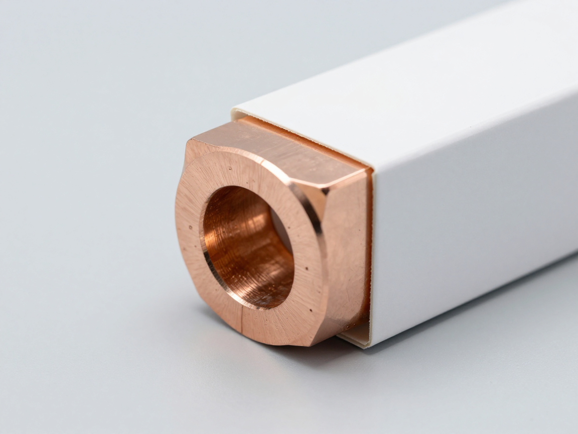
3. Types of cracks and their locations
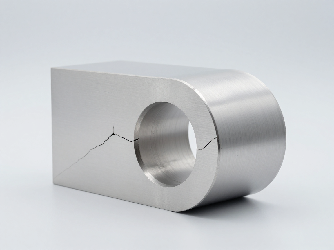
- Barrel crack: Cracks run vertically or around the wall of the seedling hole. This is the most serious form because it causes the electrical connection between the two sides of the board to be lost.
- Corner crack: appears at the transition zone between the plating layer into the hole and the pad on the surface.
- Barrel-wall separation: The plating layer is intact but separated from the base material.
- Cracks at the solder joint heel: Cracks originate from the outer edge of the fillet, usually due to mechanical stress.
- Crack between tin and component pin: signs of problems in the soldering step or in the component pin coating.
4. Distinguish the source of errors
| Signs | Highly likely origin | Need further testing |
|---|---|---|
| Cracks appeared after the thermal shock test, not before | Difference in thermal expansion between base and plating materials | Compare with samples of the same batch that have not been tested |
| Crack at the heel, with mechanical deformation around it | Assembly or handling stress | Check the procedure of plugging/unplugging and clamping the board |
| The plating layer is locally thin and has holes | Plating error in circuit board production | Measure plating thickness in many different positions |
| Many solder joints in the same area are cracked | Local heat problem or bearing area design | Compare component layout drawings |
| Cracks only appear in solder jointed joints | Repeated heat embrittles the solder joint | Check the number of re-solder joint times and heat profile |
Principle: origin conclusions must be based on at least two data sources — cross-sectional images and process or test data. Cross-sectional images alone only show the shape of the defect.
5. Tin infiltration in hole body
Tin infiltration in the hole is evaluated according to the filling level of the hole body. Need to clearly state:
- Calculation benchmark: according to board thickness or actual hole length.
- Measurement location: at the center of the hole or near the mouth of the hole.
- Double-sided condition: is the tin applied evenly to both sides of the board or just one side.
With multi-layer circuit boards, tin can also fill the inner layers. In this case, it is necessary to observe the entire length of the hole instead of just looking at the two outer sides.
6. Additional testing should be combined
- Measure hole resistance: Detection of cracks that have not yet become completely open circuit.
- Thermal shock or thermal cycling test: Apply cyclic stress to detect cracking trends.
- Vibration and bending test: Assess the effects of mechanical stress.
- Cross check with the board supplier: Compare the announced and actual plating thickness.
7. Frequently asked questions
Can cracks be seen by X-ray?
Can be seen but difficult to quantify, especially when the crack is small or located out of direction. The cross-section gives clearer information about crack location and length.
Can hole cracks be caused by the wave soldering process?
Yes, when the temperature or exposure time is not suitable. However, it is necessary to distinguish it from cracking due to thermal stress during use, because these two causes lead to different corrective actions.
Should the sample be cut before or after the thermal shock test?
You should do both: crop first to get the background image, crop later for comparison. Without a background image, it is impossible to confirm whether the crack was caused by testing or was pre-existing.
How to handle burrs in drilled holes?
Record burrs as a separate defect, evaluate the impact on plating coverage and tin adhesion. Large burrs often result in discontinuous plating in the transition zone.
Is it difficult to cut through-hole patterns on thick circuit boards?
Yes, because large hole lengths require a more precise cutting plane. You should use a suitable clamp and cut from both sides if the hole is too long.
8. Conclusion
Through-hole solder joints are subjected to many types of stress at the same time, so the crack types are also diverse and located in very different locations. Sections are the primary tool for identifying crack location and morphology, but origin conclusions must be accompanied by process or test data.
Four things to do: capture the entire length of the hole, not just both sides of the board; clearly state the benchmark for calculating tin infiltration; always have a background image before testing; and separate conclusions according to each type of stress instead of grouping them into “solder joint errors”.
References
- IPC-A-610 — Electronic assembly acceptance criteria, through-hole solder joint section.
- J-STD-001 — Requirements for electrical soldering and electronic assembly.
- IPC-6012 — Technical requirements for rigid printed circuit boards, hole-plated quality parts.
- IPC-TM-650 Method 2.1.1 — Microsectioning.
Related articles
- Why do solder joints crack after thermal shock test? Read the marks on the cross-section
- Barrel crack after assembly: causes and proof
- Cross-section solder joint: wetting angle, fillet penetration and intermetallic compound (IMC) layer
- What is Cross Section? Why do we have to cut samples to evaluate solder joints and circuit boards?
Discuss further
Disclaimer
This article is an interpretive content compiled by us; not legal advice. Enterprises need to compare relevant documents/standards verbatim before applying them to specific products.
See more: Copyright Policy & Disclaimer by ticforall.com.