

QFN and DFN are groups of components with two types of solder joints with completely different roles: pins on the side to connect the signal, and a metal base below that is both grounded and conducts heat. A product may pass in one group of solder joints but fail in another group, and the naked eye cannot distinguish.
This article guides how to read cross-sections of two groups of QFN/DFN solder joints, how to evaluate voids under the substrate and four common errors.
1. Why is QFN/DFN difficult to evaluate?
- The side legs are very short: The amount of tin forming fillets is small, making it easy to wrongly conclude that there is a lack of tin.
- The heat sink is located completely below: cannot be seen, cannot be checked by eye.
- Void under the sole does not appear: The product still works during the initial period.
- Two groups of solder joints have different criteria: same cross-section, the conclusions for the two groups may be opposite.
2. Two groups of solder joints, two sets of criteria
| Criteria | Side legs | Heatsink underneath |
|---|---|---|
| Main role | Conducting signals | Grounding and thermal conductivity |
| Characteristics to evaluate | Fillet height and width, wettability | Tin coverage level, void, solder layer thickness |
| Impact when not achieved | Signal error, weak solder joint | Local overheating, high grounding impedance |
| Severity when void is present | Low, if void is small | High, especially in the center of the sole |
| Main way to check | Visual examination, AOI, cross-section | X-ray, section |
Because the two groups have different criteria, the section report for QFN/DFN must separate conclusions for each group, not grouping them into “pass solder joint” or “fail solder joint”.
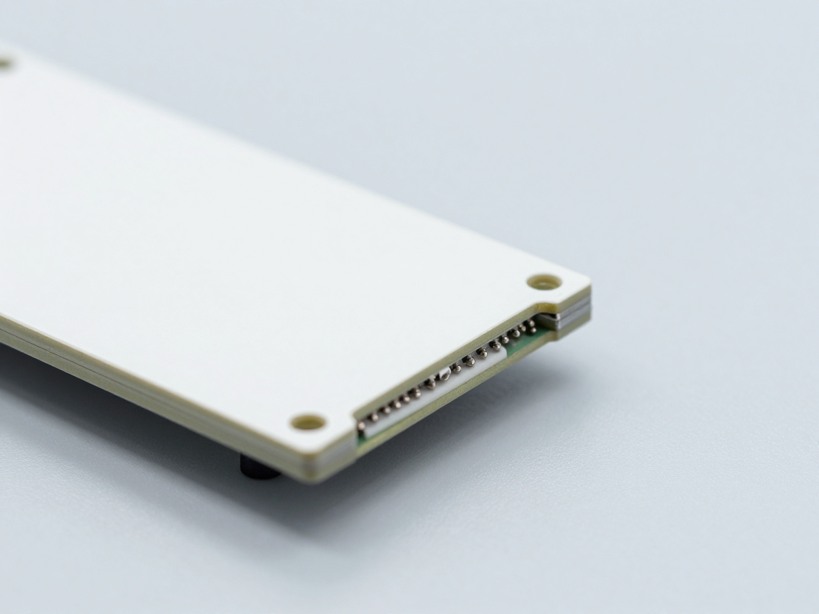
3. Read the side leg section
- Wetness: Does the tin spread evenly onto the edge of the foot and onto the pad or does it clump up?
- Fillet height: Measure from the pad surface up to the foot edge, clearly stating the landmark.
- Contact Width: Is the tin part between the foot and pad continuous or has a gap?
- Void in fillet: If so, write size and location.
A practical note: with QFN/DFN, the criteria often focus on having a metallic bond at the interface, not requiring a thick fillet. So don’t conclude an error just because the fillet is low.
4. Read the cross-section of the heat sink base
| Parameters | How to determine | Meaning |
|---|---|---|
| Tin coverage level | Ratio of tin area width to total substrate width in section | Indicates whether the tin spreads evenly across the entire substrate or is concentrated on only one side |
| Void | Record area ratio, maximum size and location | Voids in the center are more important than voids at the edges |
| Weld layer thickness | Measure at multiple points along the base | Too thin a layer increases thermal resistance |
| Link both ends | Check both the pad side and the component base side | Make sure there are no gaps at the interface |
5. Why is the void under the base dangerous?
The heat sink is the main heat escape route of the component. When there is a large void, heat cannot escape to the circuit board but accumulates in the components, leading to:
- Junction temperature is higher than design, reducing component life.
- Ground impedance increases, affecting high frequency performance.
- Thermal cycling causes voids to spread over time, causing the solder joint to deteriorate faster.
This is the reason subbase voids are often evaluated more severely than voids in signal solder joints.
6. Four common mistakes
| Error | Marks on the cross-section | Common causes |
|---|---|---|
| Tin deficiency in the hip | The tin does not cover the entire edge of the base, the interface has gaps | The amount of solder paste is not enough, the stencil opening is small, the pad is misaligned |
| Large void under the base | Large air bubble in the central area | The air cannot escape in time, the solder paste is damp, and the heat profile is not optimal |
| The tin spilled out of the base | The tin flows out of the base area and touches the adjacent area | Excess amount of solder paste, pressure on components when soldering |
| The component is lifted on one side | One side of the base has a gap, the other side is exposed | Curved circuit board, flatness deviation during soldering |
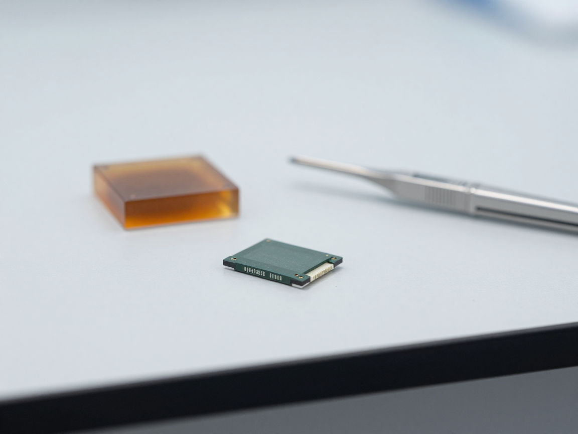
7. How to properly cut QFN/DFN samples
- Cut perpendicular to the foot row let the cross-section cut through multiple legs at the same time.
- Make sure the section passes through the center of the base to see both the center and the two edges of the base.
- Choose at least two components: one at the edge of the board, one at the middle of the board, because of different thermal conditions.
- Record the cutting direction to compare with the pinout when needed.
8. Frequently asked questions
X-ray shows void under the sole, is it necessary to cut?
Should be cut if the void is large or located in the central area. X-ray shows the scale over the entire sole; The cross-section shows which layer the void is in and the actual extent of coverage.
Is low fillet an error?
Not automatically. With QFN/DFN, the main criterion is the presence of metallic bonding at the interface. It is necessary to determine the link before concluding an error.
Are there general criteria for void under the base?
The threshold depends on the applicable standard and the heat dissipation requirements of the design. Internal thresholds should be agreed upon with the customer before assessment.
Can small DFN components be cut?
Yes, but you need to prepare the sample carefully because the area to be surveyed is small. It is recommended to use cold casting and reduce force in the polishing step.
What else should be checked besides the cross-section?
It is recommended to check the junction temperature during operation and measure the grounding impedance, because these are two indicators that reflect the actual influence of the void under the substrate.
9. Conclusion
QFN/DFN has two groups of solder joints with different roles, so they must be evaluated separately. Side pins need to confirm metal connection; The heat sink base needs to be evaluated for tin and void coverage — because this is the main heat escape route of the component.
Four things to do: cut perpendicular to the foot row and through the center of the sole; separate conclusions for two groups of solder joints; record void by scale, maximum size and position; and agree on assessment thresholds with customers before starting.
References
- IPC-A-610 — Acceptance criteria for electronic assemblies, pinless components and flat components.
- J-STD-001 — Requirements for electrical soldering and electronic assembly.
- IPC-TM-650 Method 2.1.1 — Microsectioning.
- Design and assembly instructions for components with heat sinks from the manufacturer.
Related articles
- Cross-section BGA: void measurement and head-in-pillow detection
- Cross-section solder joint: wetting angle, fillet penetration and intermetallic compound (IMC) layer
- LED cross-section and power module: intermetallic compound (IMC) layer and solder crack
- Choose the cutting position and send the cross-section sample: one wrong step and you will lose the entire data set
Discuss further
Disclaimer
This article is an interpretive content compiled by us; not legal advice. Enterprises need to compare relevant documents/standards verbatim before applying them to specific products.
See more: Copyright Policy & Disclaimer by ticforall.com.