

High-power LEDs and power modules use solder joints not only to conduct electricity but also to conduct heat. This makes their solder joint evaluation standards more stringent than conventional components: a void in an unimportant location for a signal component can be a serious problem for a power component.
This article provides instructions on reading the solder layer cross-section of LEDs and power modules, evaluating the intermetallic compound (IMC) layer thickness, identifying cracks due to thermal cycling, and how to verify reliability.
1. Why are power components different from regular components?
| Factor | Signal components | Power components |
|---|---|---|
| The role of solder joints | Conductive | Conducts electricity and heat |
| Working temperature | Low, stable | High, oscillates with on/off cycles |
| Effect of void | Mainly about mechanical durability | To both durability and heat dissipation |
| Aging rate of the intermetallic compound (IMC) layer | Slow | Noticeably faster due to long-term high temperature |
| Main type of defect | Lack of tin, misalignment | Cracking due to thermal cycling, thick intermetallic compound (IMC) layer |
2. Four characteristics to read on a cross-section
| Characteristics | Normal signs | Signs to pay attention to |
|---|---|---|
| Welding layer under the sole | Stable thickness, evenly covering the sole area | Locally thin, with tin-free areas |
| Intermetallic layer | Thin, continuous strip | Unusually thick, wavy, discontinuous |
| Void | Void is small, scattered | Large void in the center of the base — the main place of heat conduction |
| Cracks | No | Cracks run parallel to the interface or through the solder joint layer |
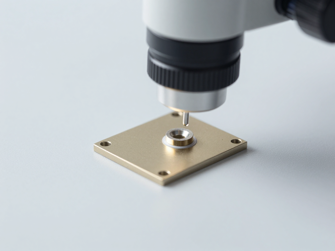
3. The intermetallic compound (IMC) layer thickens with working temperature
The intermetallic compound (IMC) layer forms immediately upon solder jointing and continues to grow over time, with the rate increasing sharply at high temperatures. With power components working continuously at high temperatures, this layer can thicken significantly over the product life cycle.
| Phase | Condition of the intermetallic compound (IMC) layer | Consequences |
|---|---|---|
| Immediately after solder jointing | Thin, continuous | Good bonding, high ductility |
| After working at medium temperature | Thickens slowly | Flexibility gradually decreases, still acceptable |
| After a long time at high temperature | Very thick, may be wavy | Brittle and prone to cracking when subjected to thermal cycles or mechanical shock |
| End of life cycle | There may be microcracking in the intermetallic compound (IMC) layer | The thermal resistance increases, the junction temperature increases, creating a deterioration spiral |
Since this process takes place throughout the product life cycle, evaluating the intermetallic compound (IMC) layer only in its initial state is not enough. Results need to be placed in the context of actual working conditions.
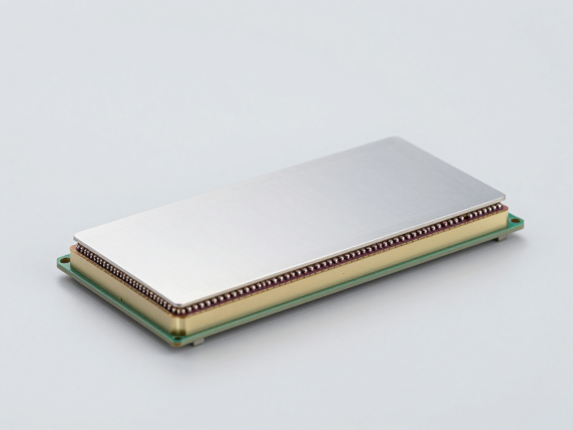
4. Void with power components
Void affects two ways, not just one:
- Thermal line: void reduces the thermal conduction cross-section, causing heat to accumulate in the component and the junction temperature to be higher than designed.
- Mechanical path: void is the stress concentration point, becoming the place where cracking begins when there is a thermal cycle.
Therefore, when evaluating voids in a power solder jointing layer, it is necessary to record all three parameters: area ratio, largest void size, and void position relative to the main heat path. Void located on the main heat path is much more serious than void at the edge.
5. Common errors and how to distinguish them
| Error | Marks on the cross-section | How to differentiate |
|---|---|---|
| Cracking due to thermal cycling | Cracks run parallel to the interface, often near the edge of the solder joint layer | Appears after the thermal cycle test, not present in the sample before the test |
| Cracking due to mechanical shock | Cracking through the solder joint layer in an oblique direction | There are traces of impact and deformation around the cracked area |
| Void concentration | Large air bubble in the soleus area | Available immediately after solder jointing, does not increase with heat cycle |
| Layering of solder jointing layers | Separation gap between two layers of tin or between tin and pad | Regarding surface contamination, present in the original sample |
| Separate classes in package | Gap inside the component body, not part of the solder joint | Observe the component body area instead of the tin area |
Important rule: to confirm cracking due to thermal cycling, there must be an untested control sample. Without a background image, the possibility of a pre-existing crack cannot be ruled out.
6. Verify reliability
- Try thermal cycling or thermal shock: Create repetitive stress to reveal cracking tendency.
- Try high power for a long time: Evaluate the evolution of the intermetallic compound (IMC) layer and the void.
- Measure junction temperature or thermal resistance: evaluate the actual impact of void on heat dissipation ability.
- Cut samples at multiple time points: before the test, between the test and after the test to see the progress.
7. Frequently asked questions
How much Void affects heat dissipation?
There is no general threshold, as it depends on heat sink design, power and junction temperature requirements. The threshold should be determined according to the thermal model of the specific product.
Is a dead LED light caused by solder joints?
Not necessarily. It could be due to the luminescent layer, the internal connection wire, or the solder joint. The cross-section helps determine exactly which floor is damaged.
Is it necessary to cut the sample after thermal cycling?
Highly recommended. This is the only way to confirm that the crack formed during the test instead of being pre-existing.
Is a thick intermetallic compound (IMC) layer always bad?
Not always, but when it exceeds a certain level, brittleness increases and reliability decreases. Need to evaluate according to the actual working conditions of the components.
Does the power module need to cut through multiple locations?
Yes. Cutting should be done in high current areas, areas near heat sinks, and edge areas — because thermal and mechanical conditions are markedly different.
8. Conclusion
With power components, the solder joint is both an electrical and thermal conductor, and that is why it ages over time. Two processes to monitor are intermetallic compound (IMC) layer thickening and void progression — both of which are difficult to detect if only examined in the initial state.
Four things to do: put the intermetallic compound (IMC) layer assessment in the context of actual working temperatures; write void according to position relative to heat path; Always have a pre-test sample as a control; and combine thermal cycling testing with thermal resistance measurements for evidence of actual effects.
References
- IPC-A-610 — Electronic Assembly Acceptance Criteria.
- J-STD-001 — Requirements for electrical soldering and electronic assembly.
- IPC-TM-650 Method 2.1.1 — Microsectioning.
- Technical documentation on thermal management and power component reliability from the manufacturer.
Related articles
- Cross-section QFN/DFN: void under the heat sink and solder pins
- Cross-section solder joint: wetting angle, fillet penetration and intermetallic compound (IMC) layer
- Why do solder joints crack after thermal shock test? Read the marks on the cross-section
- Measuring dimensions on cross-sectional images: how to set the ruler to minimize the error?
Discuss further
Disclaimer
This article is an interpretive content compiled by us; not legal advice. Enterprises need to compare relevant documents/standards verbatim before applying them to specific products.
See more: Copyright Policy & Disclaimer by ticforall.com.