

Multi-layer ceramic capacitors (MLCC) are components with a structure consisting of hundreds of ceramic layers and electrodes stacked, pressed and baked into a block. That structure allows for large capacitance in a small size, but also makes the capacitor brittle and very sensitive to board flexing forces.
The worry is that the crack inside the capacitor body may not be visible to the outside. This article guides you on reading MLCC capacitor cross-sections, identifying cracks caused by circuit board flexing and distinguishing them from delamination defects from the manufacturer.
1. Why do MLCC capacitors fail underground?
- Brittle ceramic: Good compression resistance but poor tensile and bending resistance.
- Cracks that are not visible: Cracks in the capacitor body still allow the capacitor to operate normally during the initial period.
- Progressive failure: After a while, moisture penetrates through the crack, causing electrical leakage and progressing to a short circuit.
- The location near the solder joint is the weak point: This is where the board flexing force transmitted to the capacitor body is most concentrated.
2. Four characteristics to read on a cross-section
| Characteristics | Normal signs | Signs to pay attention to |
|---|---|---|
| Electrode layer structure | The layers are evenly spaced and spaced uniformly | Misaligned layers, uneven spacing, empty areas |
| Cracks in the body | No | Cracks run through the electrode layers |
| Layering between ceramic layers | There are no gaps between layers | Gap or delamination along the interface |
| Double-ended solder joint | Fillet is even, no cracks at the junction | The crack originates from the solder joint and spreads into the capacitor body |
3. Cracks due to circuit board flexing
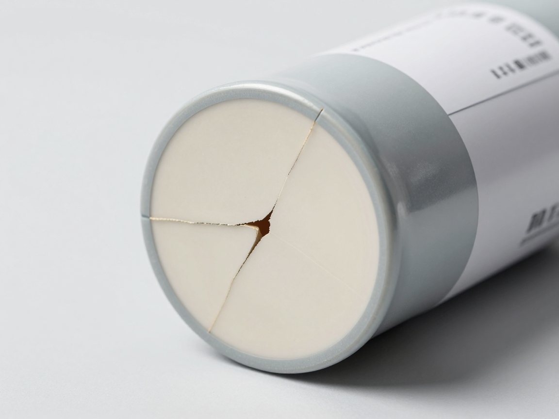
Cracks caused by circuit board flexing have a quite characteristic morphology, and identifying this morphology is the key to determining the origin:
- Starting point: usually at the condensation corner near the solder joint — where bending stress is most concentrated.
- Orchid direction: Run into the condenser body in an oblique direction, creating an angle of about 45 degrees compared to the condenser axis.
- Scope: Can cut through multiple electrode layers, creating bridges between layers.
- Secondary signs: It is common to see a slightly curved circuit board, or deformed solder joints in the surrounding area.
Mechanism: when the circuit board is bent, the hard ceramic capacitor cannot deform accordingly, so all the stress is concentrated in the area near the solder joint. Cracks form from there.
4. Distinguish from manufacturer errors
| Signs | High possibility belongs | Need further testing |
|---|---|---|
| Oblique cracks originate from the corner near the solder joint | Bending stress during assembly or use | Measure board flexing during stages; Compare how to clamp and divide the board |
| The layer separation is along the interface, regardless of the solder joint position | Classification error from capacitor manufacturing process | Check batches, compare multiple samples of the same batch |
| Empty area in class structure | Sintering or electrode printing error | Cross-section of multiple samples to confirm systematicity |
| Crack perpendicular to the capacitor axis, with burn marks at the edges | Overheating when soldering | Compare actual heat profile |
| The crack is only in the components on the circuit board, there is no separate sample | Stress from the assembly process | Compare capacitors before and after processing stages |
Principle: if the error only appears in the capacitor mounted on the board, but the separate capacitor model of the same batch has no problem, then the cause is more likely to lie in the assembly process, not in the components.
5. Additional testing should be combined
- Try bending the circuit board: Evaluate the curvature threshold that the capacitor can still withstand, according to the instructions of the applicable standard.
- Heat shock test: Detect cracks that progress with thermal cycles.
- Measure insulation resistance and leakage current: detect cracks that have not yet become a complete short circuit.
- Check the procedure of dividing the board: This is the step that creates the largest bending stress in production.
6. How to prevent in production
- Control bending force at every stage: from clamping, soldering, dividing the board to assembling.
- Arrange capacitors to avoid large bending areas: Do not place near the edge of the board or near the dividers.
- Suitable pad design: Avoid too much tin in the solder joint.
- Choose the right type of capacitor for the stressed location: There are more flexible capacitors designed for these locations.
- Check by lot and by location: Focus on high stress locations instead of random inspections.
7. Frequently asked questions
Cracked MLCC capacitors are always caused by circuit board flexing?
No. Also due to thermal shock, overheating when solder jointing, or delamination defects from the manufacturer. The morphology and location of cracks are the main basis for differentiation.
Can capacitor cracks be detected without cutting the sample?
Ultrasound scans or high-resolution X-rays can be used to suggest, but reliability is limited. Cross-section remains the confirmatory method.
Do cracked capacitors always fail immediately?
No. In many cases, capacitors still function normally and only fail after a period of time when moisture penetrates through the crack. This is why this error is difficult to diagnose late.
Can the cross-section determine when the crack formed?
Not directly. But combining cross-sectional images with process data and bending and thermal shock test results can determine which stage causes the crack.
How many capacitors should be cut per batch?
You should choose according to the location on the board: capacitors near the edge and near the dividing line, capacitors in the middle of the board, and capacitors in the vicinity of large connections. The amount depends on the risk level of the product.
8. Conclusion
MLCC capacitors fail cumulatively: cracks form in a moment but the consequences appear many months later. The cross-section is the primary tool for seeing cracks and distinguishing the source — board flexing, thermal shock, or delamination errors.
Four things to do: read the crack morphology before drawing conclusions; Compare with separate capacitor samples of the same batch; Check the stages of creating bending force; and combine bending testing with cross-sections for two-dimensional evidence.
References
- IPC-A-610 — Acceptance criteria of electronic assembly, chip components.
- IPC-TM-650 Method 2.1.1 — Microsectioning.
- J-STD-001 — Requirements for electrical soldering and electronic assembly.
- Technical documentation on bending stress and mechanical strength of multilayer ceramic capacitors from the manufacturer.
Related articles
- Cross-section small chip components 0201/0402: tombstone, insufficient solder and solder bridge
- Cross-section of crimp terminal and cable: compression, broken strands and gaps
- What is Cross Section? Why do we have to cut samples to evaluate solder joints and circuit boards?
- 10 circuit board defects can only be detected by cross-section
Discuss further
Disclaimer
This article is an interpretive content compiled by us; not legal advice. Enterprises need to compare relevant documents/standards verbatim before applying them to specific products.
See more: Copyright Policy & Disclaimer by ticforall.com.