A cross-section sample set is only valuable when the cutting position correctly answers the question at hand. Cutting in the wrong place, even though the photo is very sharp and the measurements are very accurate, is still inconclusive — and once the model is destroyed, it cannot be remade.
This article provides instructions on how to determine cutting positions according to analytical goals, how to sample in batches, how to mark and orient samples, and the required information that must be included.
1. The question of deciding where to cut
The correct order is always: determine the question first, choose the cutting location later. Doing the opposite — cutting first and then thinking about what to ask — is the most common cause of having to take a second sample.
| Questions need answering | Cutting position | Key criteria |
|---|---|---|
| Is the plating thickness in the hole satisfactory? | Holes in many different positions on the panel | Plating thickness at hole wall |
| Is the solder joint a real connection? | Along the solder joint joint to be inspected | Wetting angle, absorbency, intermetallic compound (IMC) layer |
| Does BGA have large voids? | Through the row of marbles at the center and edge positions | Void size and distribution |
| Is the circuit board misaligned? | Panel edge area and middle panel area | Number of layers, bias, dielectric thickness |
| Is the drill hole cracked? | The correct hole has increased resistance, along with the control hole | Continuity of the plating layer |
| Does the crimp terminal compress enough? | Along the body of the crimp terminal, keep the pressure area intact | Compression, void, broken string rays |
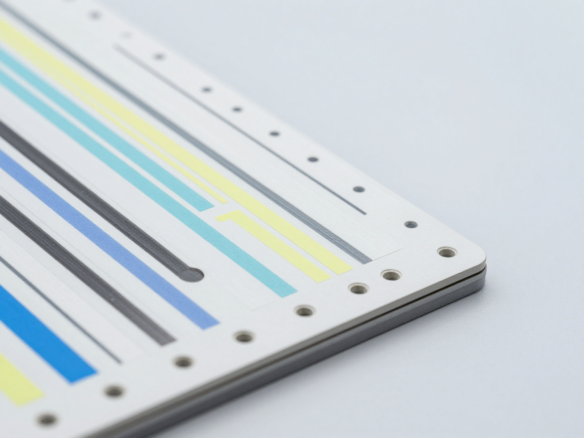
2. Four principles for choosing cutting locations
- Representative: For questions about batch capacity, sample from multiple locations (edges, middle, high-density areas) instead of multiple samples from the same location.
- There is evidence: Always take another passing sample for comparison. Control images help distinguish real abnormalities from normal characteristics of the sample.
- Right direction: The cutting plane must be perpendicular to the axis to be surveyed. Cutting diagonally will make any measured thickness larger than it actually is.
- Keep backup samples: For important samples, keep an intact portion of the same part so you can cut again if the first attempt fails.
3. Batch sampling: three common ways
| How to take samples | How to do it | Advantages | Limitations |
|---|---|---|---|
| Coupons are pre-designed on the panel | Use the coupon area attached to the panel that the designer has reserved | Does not affect the product; Fixed location should be comparable between batches | Not all designs have coupons |
| Sample from panel edge area | Cut out the non-functional area at the edge of the panel | Take advantage of the waste, save money | It is necessary to check whether the boundary conditions are the same as the middle area or not |
| Sample from real product | Directly cut the product or assembled circuit board | Correctly reflects production conditions | Loss of product; Need a legitimate reason |
Practical recommendations: use coupons for periodic monitoring, use real products when analyzing problems — because then the question is no longer “is the procedure stable” but “what happened to this product”.
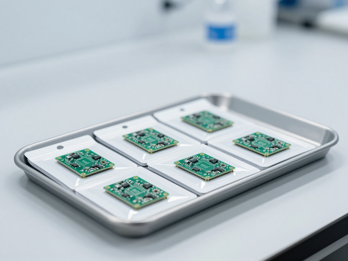
4. Mark and orient the sample
| Things to do | How to do it | Why is it important? |
|---|---|---|
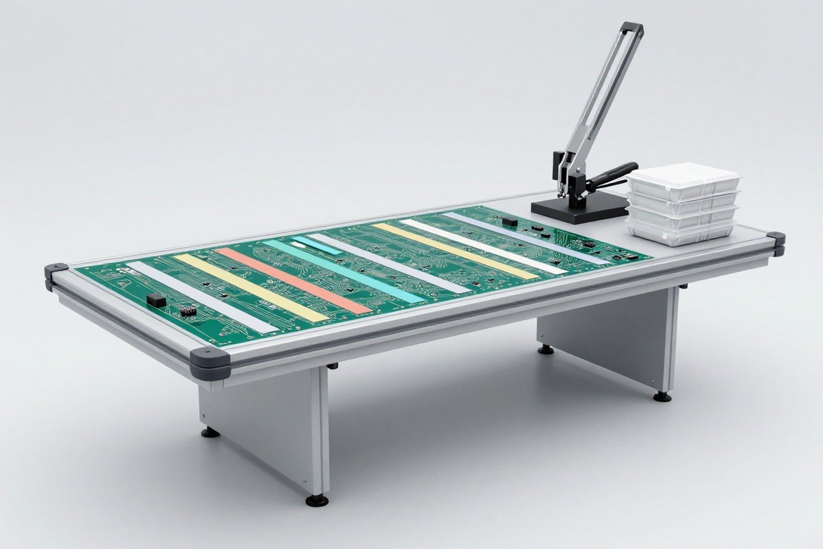
| Mark the cutting plane | Use colored tape or an oil pen to draw a cutting line on the outside of the template | Avoid misdirection once the sample has left the factory |
| Record arrow direction | Draw an arrow pointing from which edge, going in which direction | The section must maintain the correct direction for comparison with the drawing |
| Write down the identification code | Lot code, board code, date, location symbol | Without the code, the data set loses its ability to be retrieved |
| Do not write on the area to be examined | Only write on the opposite side or outside the survey area | Pen ink and glue can eat into the surface to be analyzed |
5. Packaging and transportation
With assembled models, the two main risks are impact and moisture:
- Wrap each sample individually in an anti-static bag or sealed plastic bag, with a code slip in the bag.
- Fix the sample so that the part to be analyzed does not come into contact with other materials.
- If the area to be investigated has a small solder joint, it should be fixed with a stand instead of letting the sample lean against each other.
- Add a desiccant package when transporting long distances or during the rainy season.
If the sample is a circuit board that has been tested for corrosion or humidity, this condition must be clearly stated in the submission form: the corrosion results on the cross-section depend greatly on how the sample is preserved after the test.
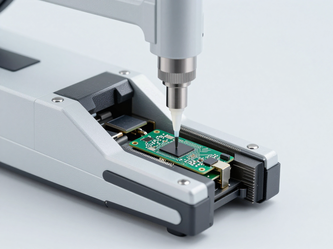
6. Mandatory information attached
- Specific questions need answering.
- Batch code, product code and manufacturing date.
- Cut location and desired cutting direction.
- Standards and product classes apply for evaluation.
- Related design requirements (desired plating thickness, hole diameter, number of layers).
- History of the sample: any tests passed, any known abnormalities.
- Control sample (if any).
- Technical contact information to discuss when clarification is needed.
7. Frequently asked questions
Can I send a whole panel instead of a pre-cut sample?
Yes, and in many cases this is a better way: the test room will choose the cutting position according to the question. The condition must clearly state the request and indicate which parts cannot be cut.
Can a sample that breaks along the cut line still be used?
Usually not, because the broken edge distorts the layer to be measured and creates false defects. It is necessary to keep the sample intact until cutting with specialized equipment with cooling.
How many positions should be cut for a routine check?
There should be a minimum of three different positions representing different risk areas on the panel, rather than three adjacent samples.
Do samples that have passed the thermal shock test need to be sent with samples that have not been tested?
There should be. The “tested – not tested” sample pair is the only way to distinguish pre-existing errors from errors that arise during testing.
Should we take photos of samples before sending?
So, especially with samples that have visible abnormalities. Photos before sending help compare and avoid arguments about sample condition at the time of delivery.
8. Conclusion
Choosing the cut location is the cheapest but most influential step in the entire cross-section process. The question determines the position, the position determines the measurement criteria, and the measurement criteria determines the value of the conclusion.
Four things to do: always have a control sample; Sampling at many different locations when evaluating batch capacity; Mark the cutting direction clearly; and include specific questions and complete retrieval information.
References
- IPC-TM-650 Method 2.1.1 — Microsectioning, site selection and sample preparation.
- IPC-A-600 and IPC-6012 — Printed circuit board technical requirements and acceptance criteria.
- IPC-A-610 — Electronic Assembly Acceptance Criteria.
- Instructions for sampling and sample retrieval in the testing laboratory quality management system.
Related articles
- Cross-section in aviation and military: request records and retrieval
- IPC-TM-650 2.1.1: standard microsection procedure
- Two Laboratories, Two Different Results: Why?
- 5 strange marks on the cross-section: distinguish real errors from phenomena due to sample preparation
- Barrel crack after assembly: causes and proof
- Cross-section of crimp terminal and cable: compression, broken strands and gaps
- Cross-section QFN/DFN: void under the heat sink and solder pins
- From rough samples to cross-section images: casting, grinding, polishing and etching
- Measuring dimensions on cross-sectional images: how to set the ruler to minimize the error?
- 7 situations where factories are forced to do cross-sections
- What is Cross Section? Why do we have to cut samples to evaluate solder joints and circuit boards?
Discuss further
Disclaimer
This article is an interpretive content compiled by us; not legal advice. Enterprises need to compare relevant documents/standards verbatim before applying them to specific products.
See more: Copyright Policy & Disclaimer by ticforall.com.