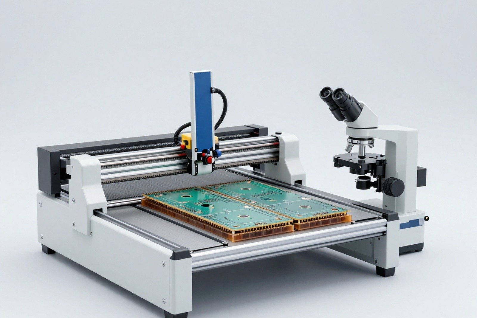
Barrel crack is a type of damage in which the coating in the hole is broken longitudinally or circularly. What makes it difficult to handle is the timing of its appearance: the product passes the output test, passes the function test, but it is not until the final assembly stage or even after delivery that a connection loss error occurs.
This article guides you on how to read cracks and holes on cross-sections, distinguish the origin and how to prove where the error arose.
1. Why do cracks appear after assembly?
The in-hole plating is a thin metal tube that penetrates the substrate material. When the board is bent or subjected to mechanical force, this plated tube is the place where the greatest stress is concentrated because it is harder than the surrounding material but the cross-section is small.
| Assembly stage | How to create stress | Risk level |
|---|---|---|
| Divide the circuit board into small panels | Bending force and vibration force when cutting or breaking | High — this is the most dangerous step |
| Clamps, fixtures | Uneven pressure on the board surface | On average, depends on the fixture |
| Screw and screw into the bracket | Local traction around the screw position | High if the screw is located near the plated hole |
| Bend the board to fit it into the case | Horizontal bending force through multiple plated holes | High for products with small shells |
| Plug and unplug the connector | The force is transmitted through the component pin down to the plated hole | Medium to high depending on frequency |
| Tighten the cable and tie the rope | Continuous pulling force on the connection point | Average, but cumulative over time |
Important point: mechanical stress does not cause immediate cracking. It creates cumulative microcracks, and each time the board is bent, the crack spreads a little further. This is the reason the error appears late.
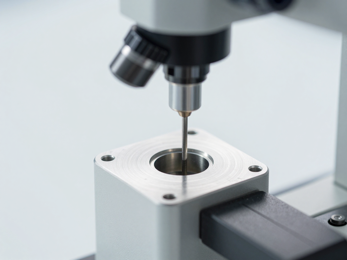
2. Marks to be read on the cross-section
| Traces | Meaning | What needs to be recorded? |
|---|---|---|
| Crack location by depth | Crack in the middle of the hole or near the mouth of the hole | Distance from board surface to crack |
| Crack direction | Around the hole or vertically | Describe the morphology, not just “cracked” |
| Number of cracks | One mark or many marks in the same hole | Draw a diagram of the relative positions of the spots |
| Extent of spread | Whether or not the crack has cut through the entire thickness of the plating? | Calculate the percentage of broken cross-section |
| Surrounding condition | The base material may separate from the plating, have voids, and show signs of deformation | Description of auxiliary traces |
Practical note: if the crack is located in the transition area between the plating layer and the pad on the surface, it is a corner crack. If the crack is in the middle of the hole body depth and runs around, it is usually the result of board flexing stress.
3. Distinguishing origins
| Signs | High possibility belongs | Need further testing |
|---|---|---|
| Circular crack in the middle of the depth, many holes in the same affected area | Board bending stress in assembly | Processes that involve bending or breaking circuit boards |
| Cracks appear in holes near the edge of the board or near the dividing line | Mechanical force when dividing the plate | Division method, tools, hole placement |
| Cracked thread in hole that has been re-soldered many times | Repeated heat reduces the ductility of the plating and intermetallic | Number of re-solder jointing times, heat profile |
| Locally thin plating, with flaws from the beginning | Plating quality of the board | Declared plating thickness, check bare board |
| Cracks in the same location on many different lots | Design issues or repeatable processes | Hole design, materials, assembly process |
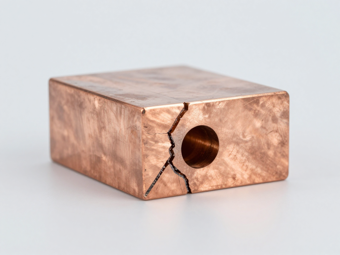
4. How to prove at which stage the error occurs
Principle: must capture the state of the sample after each step, instead of just comparing input with output.
- Sampling at multiple points along the line: after solder jointing, after dividing the panels, after installing into the shell, before packaging.
- Cut the sample at each point: at least three samples per point to eliminate random variation.
- Compare the same hole position: Must cut at exactly the same hole in samples with different points, otherwise comparison will not be possible.
- Record process parameters: clamping force, board placement, plate dividing tool, screw tightening torque.
- Conclusion according to the data: If the sample after stage A does not have cracks, but after stage B it already exists, then stage B is the main candidate.
It’s a time-consuming process, but it’s the only way to move from speculation to evidence — and evidence is essential when talking to customers or suppliers.
5. Additional testing should be combined
- Measure hole resistance using the four-wire method: Detect cracks that have not yet become completely open circuits, thereby detecting errors earlier.
- Try three-point bending: reproduce mechanical stress in a controlled environment.
- Vibration test: Assess cumulative effects over operating time.
- Check the bare circuit board before soldering: eliminate the possibility of a plating error available from the board supplier.
6. Frequently asked questions
Is the crack in the hole the fault of the board supplier?
Only when the thickness or plating quality is below standard. If the plating meets standards but still cracks, the cause often lies in mechanical stress during assembly or use.
How to detect early without having to cut many samples?
Use the four-wire hole resistance measurement in the first batch to find holes that tend to increase resistance, then cut only those holes. This method reduces the number of samples that have to be cut while still having the focus.
Should I test the circuit board before shipping?
For products with high-risk of stress, there should be a bending test according to applicable standards. This test helps detect cracking trends before the product leaves the factory.
If just a few holes are cracked, is it serious?
Have. A crack can cause a complete loss of connection and lead to product failure. For products with high safety requirements, the acceptance threshold is often very strict.
Does solder jointing temperature cause cracks in holes?
It is possible, if the heat is too high or the exposure time is too long, and can also cause cracking other than mechanical stress cracking. It is necessary to compare both thermal profiles and assembly conditions.
7. Conclusion
Hole cracking is a cumulative error, so the time of detection is often far from the time of formation. To determine the origin, samples must be taken at each stage and compared at the same hole location.
Four things to do: localize the steps that create bending or tensile forces; Cut the sample according to the stage mark in exactly one hole; measure four-wire hole resistance to get quantitative data; and only conclude the origin when there is two-way evidence.
References
- IPC-6012 — Technical requirements for rigid printed circuit boards, hole plating reliability section.
- IPC-TM-650 Method 2.1.1 — Microsectioning.
- IPC-TM-650 — Bending and thermal cycling test methods.
- IPC-A-610 — Electronic assembly acceptance criteria, through-hole solder joint section.
Related articles
- Cross-section through-hole solder joint: when does the pin solder joint crack?
- Why do solder joints crack after thermal shock test? Read the marks on the cross-section
- From cross-sectional image to root cause: 5 investigation steps
- Choose the cutting position and send the cross-section sample: one wrong step and you will lose the entire data set
Discuss further
Disclaimer
This article is an interpretive content compiled by us; not legal advice. Enterprises need to compare relevant documents/standards verbatim before applying them to specific products.
See more: Copyright Policy & Disclaimer by ticforall.com.