Thermal shock testing is a common test to evaluate the reliability of solder joints. But when a sample cracks after testing, the important question is not “whether there is a crack” — but “was the crack created by the test, or was it pre-existing and only revealed when subjected to stress”.
This article provides instructions on reading crack marks on a cross-section after a thermal shock test, distinguishing cracks caused by testing from pre-existing cracks, and how to design a test to have a certain conclusion.
1. Why does thermal shock testing cause cracked solder joints?
In a solder joint, there are many materials with different levels of thermal expansion: circuit board base material, copper plating, solder, and component body. When the temperature changes rapidly, these materials do not expand at the same rate, creating concentrated stress at the transition points.
| Mechanism | How to create stress | The location is often cracked |
|---|---|---|
| Expansion difference between base material and metal | Metals and base materials expand and contract differently when the temperature changes | Plating hole wall, interface between plating and material |
| Expansion difference between components and circuit boards | The component body and circuit board do not stretch at the same time | Weld corner, near the edge of the component |
| Brittle intermetallic compound (IMC) layer | The intermetallic compound (IMC) layer thickens due to high temperature, reducing ductility | Interface between tin and pad |
| Gap or void available | Gaps and voids are stress concentration points | Right at the gap or at the edge of the void |
Point to remember: the first three mechanisms are design or process causes, while the fourth mechanism only exposes a pre-existing defect. Cross-section helps distinguish these two groups.

2. Five marks to read on the cross-section
| Traces | Tell me what |
|---|---|
| Crack location | Located in the tin, at the interface, in the plating layer, or in the base material |
| Crack direction | Parallel interface suggests shear stress; skewing through the tin block suggests tensile stress |
| Relative length | What percentage of the solder joint cross-section is cracked? |
| Crack edge | Sharp, clean edges suggest new cracks; Oxidized edges or impurities suggest cracks that have been present for a long time |
| Secondary marks around the crack | There is plastic deformation, secondary cracks, or adjacent voids |
The fourth trace is the most important fact to distinguish new cracks from old cracks. An oxidized crack edge indicates that the crack has existed long enough for the surface to be exposed to air — meaning it formed before the test.
3. Distinguish between test cracks and existing cracks
| Signs | High possibility of cracking due to testing | There is a high possibility that cracks are present |
|---|---|---|
| Crack edge | Clean, not oxidized | There is an oxidation layer or impurities |
| Appears in many samples at the same time | Yes, related to general stress | Just a few samples, no rules |
| Location | Concentrated at the material transition point | Any, related to local defects |
| Deformation traces | Yes, due to high stress | Little or none |
| Pre-test sample | No cracking | There was a crack in the same location |
The final signal — comparison with the pre-test sample — is the strongest evidence. Without a background image, any conclusions about the cause are speculative.
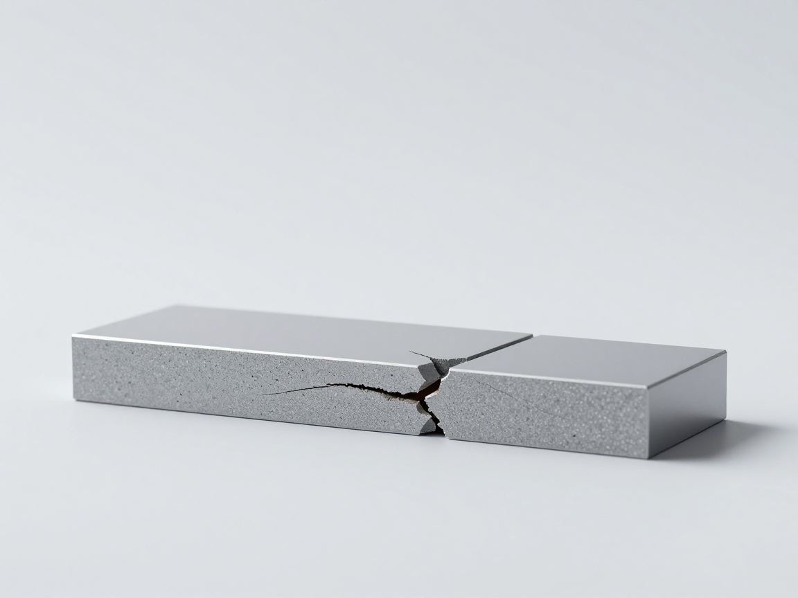
4. Note: errors in sample preparation can easily be mistaken for real cracks
Cutting and grinding the sample can also create marks that look like cracks. Easily confused forms:
- Scratches due to abrasive particles: parallel, even lines, usually located on the surface.
- Cracking due to shear force: appears at the edge of the sample, in the direction of the cutting edge.
- Pulled metal burrs: long, thin metal strip that runs along the grinding surface.
- False gap due to sample pitting: voids form when the casting material is not completely absorbed.
How to distinguish: real cracks usually have a direction related to the solder joint structure and penetrate deeply into the material, while cracks caused by sample preparation are usually located in the surface layer and do not follow stress logic.
5. How to design a trial to get solid conclusions
- Cut the sample before testing: This is a mandatory, irreplaceable comparison benchmark.
- Record actual thermal profile: temperature, time, number of cycles, heat transfer rate.
- Cut samples at many landmarks: after few cycles and after many cycles to see the rate of progress.
- Select model by location: components at the edge of the board, in the middle, and near areas of high thermal mass.
- Keep control samples: same batch, not tested, to eliminate existing errors.
6. Frequently asked questions
Is cracking after thermal shock test a fault of the solder jointing process?
Not necessarily. Can be a consequence of design (material selection, component placement), solder jointing profile, or pre-existing defects. It is necessary to read the trace and compare it with the background sample.
What does the crack pattern in the first cycle mean?
Usually suggests a pre-existing defect or serious material problem. It is necessary to check the sample before testing the same batch to confirm.
Should I cut the sample immediately after testing or let it cool and then cut?
The sample should be brought to room temperature before cutting, to avoid causing additional stress. Clearly state the cutting time compared to the end of the test.
How to distinguish test cracks from grinding scratches?
Scratches caused by grinding are usually parallel, even and only on the surface. Stress cracking is structurally oriented and penetrates deep into the material. If you are not sure, you should grind again and observe at a deeper layer.
How many cycles is enough?
Depending on applicable standards and assessment objectives. It is important to clearly state the actual number of cycles and always have a control sample for comparison.
7. Conclusion
After thermal shock testing, cracks are data, not conclusions. To know the cause of the crack, you must read its location, direction, edges and secondary traces — then compare it with the pre-test sample.
Four things to do: always cut samples before testing; record actual thermal profile; Observe the edge of the crack to evaluate whether it is new or old; and eliminate the possibility of fake stains due to sample preparation before conclusion.
References
- IPC-TM-650 — Test methods, thermal shock and thermal cycling test sections.
- J-STD-001 — Requirements for electrical soldering and electronic assembly.
- IPC-TM-650 Method 2.1.1 — Microsectioning.
- IPC-A-610 — Electronic Assembly Acceptance Criteria.
Related articles
- Barrel crack after assembly: causes and proof
- From cross-sectional image to root cause: 5 investigation steps
- Cross-section through-hole solder joint: when does the pin solder joint crack?
- Measuring dimensions on cross-sectional images: how to set the ruler to minimize the error?
Discuss further
Disclaimer
This article is an interpretive content compiled by us; not legal advice. Enterprises need to compare relevant documents/standards verbatim before applying them to specific products.
See more: Copyright Policy & Disclaimer by ticforall.com.