

A conformal coating exists to block moisture, dust, and impurities from the circuit board surface. But when the coating doesn’t adhere well enough, it not only loses its protective effect — it also becomes a permanent site for moisture and impurities on the surface, causing the condition to deteriorate more quickly than if left uncoated.
This article provides instructions on how to read peeling coating and pad peeling marks on cross-sections, how to distinguish the origin, and what control points are needed in production.
1. Why does the coating peel off?
Coating adhesion depends on three factors: whether the surface is clean, whether the surface is dry, and whether the coating has cured properly. Without any of these elements, the coating may still look normal when first applied but gradually peel off over time.
| Cause | Mechanism | Marks on the cross-section |
|---|---|---|
| Surface contamination | Impurities prevent the coating from coming into direct contact with the surface | The coating is located a thin distance from the surface, with a strange streak in the middle |
| Moisture remains on the surface | Moisture rises during solidification, creating air pockets or reducing adhesion | Small bulges or gaps along the interface |
| Freezing snakes is not enough | The coating is still soft and can easily be cut or pulled off the surface | The coating deforms, the peeling edges stretch into fibers |
| Mechanical stress after coating | Shear or tensile forces from the assembly act on the edge of the coating | Flaking starts from the edge or from the edge of the component |
| Incompatible materials | The coating has a different expansion rate than the base material, separating according to thermal cycles | Extensive flaking, in the direction of thermal stress |
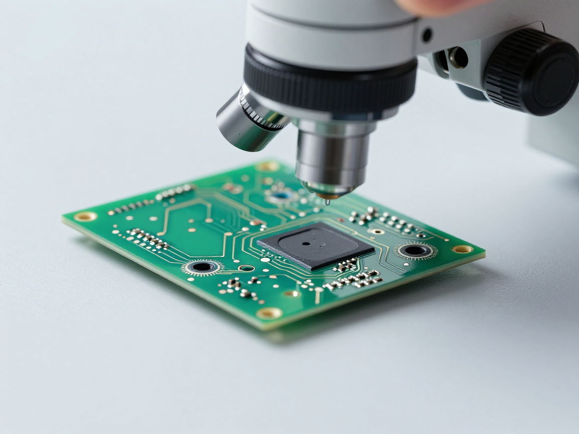
2. Types of bubbles and how to identify them
- Edge peeling: The coating separates from the surface starting from the edge or from the edge of the component. This form is often due to mechanical force.
- Wide area: The coating separates into large patches, often related to thermal stress or residual moisture.
- Local flaking on the solder joint: The coating separates from the tin surface but remains attached to the surrounding base material, usually because the tin surface has an oxide layer or flux residue.
- Air pockets under cover: closed space between the coating and the surface, not completely separated but still creating a moisture path.
- Flange according to component leg area: The coating separates around the base of the component, creating a gap that conducts moisture directly to the solder joint.
3. Marks to be read on the cross-section
| Traces | Meaning |
|---|---|
| Coating thickness according to location | Identify unusually thin areas, this is where the protection is weakest |
| Contact state at the interface | Distinguish whether the coating is located close to the surface or away from a gap |
| The material is in the gap | If there are impurities, it is evidence that the surface has not been cleaned |
| Peeling starting position | Start from the edge, from the component edge, or from any other point |
| Cracks in the coating | Cracking of the coating also creates moisture paths even though the coating does not peel off the surface |
4. Pad peeling and substrate material cracking
A related but more serious form of damage is pad shedding: the copper pad separates from the backing material, or the backing material cracks just below the pad. Two common mechanisms:
- Excessive traction: When removing components, pulling wires or tightening connectors, force is transmitted to the pad and separates it from the material.
- Cracking of the base material just below the pad: This form does not cause the pad to completely separate but weakens the bond, leading to an open circuit when additional thermal stress is applied.
On the cross-section, the second form is harder to see because the pad is still in the correct position. The telltale sign is a crack in the base material running just below the edge of the pad — which should be observed closely with high magnification.
5. Effects when the coating loses its effectiveness
| Influence | Mechanism | Expression |
|---|---|---|
| Moisture and impurities accumulate | The gap between the coating and the surface becomes the path | Corrodes metal surfaces over time |
| Electrical leakage between two close points | Conductive impurities in the gap create conductive paths | Leakage current increases with environmental humidity |
| Electrochemical corrosion | Moisture combined with voltage creates a corrosive reaction at the connection | Metal corrodes, contact resistance increases |
| Reduces the mechanical strength of the solder joint | Corrosive materials weaken the solder joint | Cracking appears after many environmental cycles |
6. Control points in production
- Clean the surface before coating: This is the most important step and also the most overlooked.
- Control residual moisture: Dry at appropriate time and temperature before coating.
- Make sure it is fully frozen: Check the curing time and temperature according to the material manufacturer’s recommendations.
- Avoid mechanical stress after coating: Check whether the post-coating steps accidentally impact the edge of the coating.
- Periodic inspection by cross-section: Conventional adhesion tests do not detect air pockets under the coating.
7. Frequently asked questions
Is peeling coating always the fault of the coating material?
No. The most common cause is that the surface has not been cleaned properly or is still damp before coating. It is necessary to check the procedure before changing materials.
Is there a way to test adhesion without cutting the sample?
There are surface adhesion tests, but they only evaluate the coating at the test site, not detecting air pockets or local gaps underneath. The cross-section adds that information.
Are air pockets under the cover always at fault?
Not immediately. But it is a potential moisture conduit, and in highly humid or contaminated environments, it becomes a corrosion initiation point.
Can a bong pad be detected by normal testing?
Only when the pad has separated is visible. In cases where cracks in the substrate material under the pad are often not apparent, a cross-section or resistance test must be used.
Where should I focus on cutting?
You should choose areas with many pin components, the interface between the coating and the component pin, and the area near the connector — places that are most exposed to mechanical and moisture impacts.
8. Conclusion
The coating is only effective when it truly adheres to the entire surface. A small gap is enough to turn the protective layer into a permanent moisture trap, and the consequences appear late in the form of corrosion and electrical leakage.
Four things to do: control cleaning and drying before coating; Check the cross-section in the first batch to see air pockets and gaps; clearly state the location of the start of peeling to deduce the stress source; and incorporate environmental testing to assess actual effects over time.
References
- IPC-A-610 — Acceptance criteria of electronic assemblies, protective coating section.
- IPC-CC-830 — Standard for protective coating materials for printed circuit boards.
- IPC-TM-650 Method 2.1.1 — Microsectioning.
- J-STD-001 — Requirements for electrical soldering and electronic assembly.
Related articles
- What is Cross Section? Why do we have to cut samples to evaluate solder joints and circuit boards?
- 5 strange marks on the cross-section: distinguish real errors from phenomena due to sample preparation
- 10 circuit board defects can only be detected by cross-section
- Cross-section of crimp terminal and cable: compression, broken strands and gaps
Discuss further
Disclaimer
This article is an interpretive content compiled by us; not legal advice. Enterprises need to compare relevant documents/standards verbatim before applying them to specific products.
See more: Copyright Policy & Disclaimer by ticforall.com.