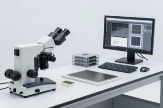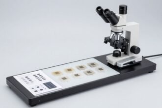

Every electronic component has a structural part that no camera, no X-ray, and no human eye can see: the thickness of the plating layer inside the hole wall, the penetration of tin into the component pins, the intermetallic compound (IMC) layer formed between tin and copper. If you want to know those things, you have to cut out the sample.
This article explains what a cross-section is, why it is the only method that can answer a specific set of questions, what the sample preparation process entails, and four limitations to be aware of before using the results to draw conclusions.
1. What is cross-section?
Cross-section (also known as cross-section, microsection) is a method of cutting a sample – circuit board, solder joint, connector, cable – through the correct position to be investigated, molding the sample into a plastic mold, grinding and polishing the cross-section to the necessary flatness and gloss, then observing under an optical microscope or electron microscope.
Core principle: section creates a two-dimensional “slice” of a three-dimensional structure. Everything lying on the cutting plane is visible; anything that deviates from that plane is ignored. This is both the strength and the biggest limitation of the method.
2. Why do we need to cut samples? What is outside cannot be told
| Question | Visual inspection/AOI | X-ray | Cross-sections |
|---|---|---|---|
| Thickness of plating layer in hole | Can’t see | Cannot be measured | Measure directly |
| Tin absorption on component pins | Only the exposed part is seen | Just see the overall shape | See the entire solder joint cross-section |
| Intermetallic layer between tin and copper | Can’t see | Can’t see | Visible and measurable |
| Cracks inside the hole wall | Can’t see | Can be seen but difficult to quantify | Clearly see position and length |
| Separation between layers of material | Can’t see | Limitations | See clearly |
| Hole and annular ring concentricity | Only the top is visible | Cannot measure accurately | Measurable |
In short: the cross-section answers questions about inside size and Bond quality between material layers. That is a group of questions that non-destructive methods can only suggest, not confirm.
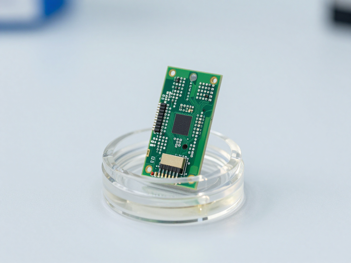
3. Six indicators can only be measured by cross-section
- Hole plating thickness: determines the electrical conductivity and mechanical strength of the drill hole.
- Surface coating thickness: Chemical or electroplated layer on the pad, directly affects solder jointing ability.
- Fillet and wetting angle: Indicates whether the solder joint has formed a real bond or is just surface-attached.
- Intermetallic layer thickness: too thin and the bond is weak, too thick and it’s brittle — this is the long-term reliability factor.
- Void and layer separation: Determine the location, size and density of internal defects.
- Layer deviation and number of layers: Check if the multi-layer circuit board is of the correct design or if it is misaligned during the pressing process.
4. Sample preparation process: five steps that determine image quality
| Step | Purpose | Common errors |
|---|---|---|
| Cut the pattern | Create a preliminary cross-section through the correct location to be surveyed | Choosing the wrong location; The heat generated deforms the sample |
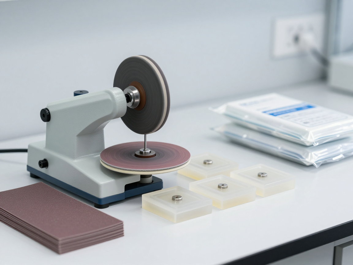
| Casting samples | Holds the sample in place and protects the cut edge | The molding is not tight, the plastic flows into the gap, causing the edge of the sample to be distorted |
| Rough grinding | Flatten the section, bringing the sample to the correct plane to be examined | Grinding too much will cause the part to be examined to be lost |
| Polishing | Removes scratches and surface deformation layers | Ignore the grain level, leaving the deformation layer covering the structure |
| Corrosion (if necessary) | Increase contrast between phases and material layers | Too strong corrosion causes loss of small details |
Point to emphasize: in reality, the majority of unsatisfactory cross-sectional images are caused by sample preparation, not by the microscope. A normal microscope with a well-prepared sample produces much better images than a high-end microscope with a scratched or chamfered sample.
5. Reading cross-sectional images: four groups of features to look at
- Thickness: plating layers, dielectric layers, coatings — measured and compared to design requirements.
- Interface shape: Is the solder joint evenly wetted, has a concave corner, is there a gap between the tin and the component pin?
- Disability: void, crack, delamination, impurities, misalignment — note location and size.
- Crystal structure: particle size, intermetallic compound (IMC) layer morphology, signs of overheating or cooling too quickly.

6. When do you need to do a cross-section, when do you not need to?
| Situation | Is cross-section needed? | Reason |
|---|---|---|
| Confirm the new supplier’s board batch | Yes, in the first lot | Measure plating thickness and drill hole quality |
| Rapid screening for the presence of restricted substances | No | Use the more appropriate elemental screening method |
| The solder joint joint cracked after the thermal shock test | Yes | It is necessary to determine the location and mechanism of cracking |
| Inspect 100% of products on the line | No | Destructive method, not for use on entire batches |
| Customer complaints about solder joint deformation | Yes | Prove the internal structure with photos |
| Evaluate new designs before mass production | There should be | Detect design errors before they become costly |
7. Four limitations of the method
- Sample destruction: Cut samples cannot be returned to the line. The cost therefore includes the sample value.
- Only see one plane: Defects located outside the section will not appear in the image. The conclusion “no error seen” is only true for the cut plane.
- Depends on the operator: For the same sample, two technicians may give different images and measurements if the procedure and definition of measuring points are different.
- Limited models: It is not possible to cut the whole lot, so the results are always conclusions on the sample, which need to be placed in the context of sampling.
8. Frequently asked questions
Are cross-sections and microsections different?
In actual usage, the two words are often used interchangeably. “Microsection” emphasizes observation at microscopic magnification, while “cross-section” emphasizes cutting through structures. There should be a unified name in the file to avoid misunderstandings.
Is it possible to do a cross-section without destroying the pattern?
No. The essence of the method is sample cutting. However, damage can be reduced by choosing the cutting location in a permissible area (eg coupon area or non-functional edge area) if the design takes this into account.
How many samples are needed for one assessment?
Depends on goals and risk level. With a new batch from a new supplier, samples should be taken from many different locations on the panel instead of multiple samples from the same location.
Can a cross-section be used to draw conclusions for the whole lot?
Only if sampling and number of samples permit. A cross-section represents a point; Conclusions for the whole batch require sample sets and corresponding statistical arguments.
Is cross-section necessary for all types of products?
No. For products without solder joints or without a multi-layer structure, the value of the method will be low. It is most valuable for multi-layer boards, hidden solder joints, and metal interconnects.
9. Conclusion
Cross-section is the only method that looks directly at the internal structure of the solder joint and circuit board: plating thickness, tin penetration, intermetallic compound (IMC) layer, voids and delamination. It does not replace non-destructive methods but complements them in the group of questions of size and material bonding.
Three things to do: determine the questions that need to be answered before choosing a cutting location; Invest in sample preparation because that is the deciding factor in photo quality; and clearly state in the report that the conclusions are related to the cutting plane and specific sample set.
References
- IPC-TM-650 Method 2.1.1 — Microsectioning, procedure for preparing cross-sectional samples for printed circuit boards.
- IPC-A-600 — Printed circuit board acceptance criteria, cross-section evaluation.
- IPC-6012 — Technical and performance requirements for rigid printed circuit boards.
- IPC-A-610 and J-STD-001 — Weld acceptance criteria and solder jointing material requirements.
- ASTM E3 — Guide to metallographic sample preparation; ASTM E407 — Corrosion of metals.
Related articles
- Cross-section in aviation and military: request records and retrieval
- Cross Section in Automotive and Medical Devices: How the Requirements Differ
- IPC-7095: void criteria for level-specific BGA
- J-STD-001 and IPC-A-610: evaluation of solder joints through cross-section
- IPC-TM-650 2.1.1: standard microsection procedure
- IPC-A-600 and IPC-6012: cross-section board acceptance criteria
- Two Laboratories, Two Different Results: Why?
- 5 strange marks on the cross-section: distinguish real errors from phenomena due to sample preparation
- From cross-sectional image to root cause: 5 investigation steps
- Peeling of coating and loss of veins: read traces on cut surface
- Barrel crack after assembly: causes and proof
- Why do solder joints crack after thermal shock test? Read the marks on the cross-section
- 10 circuit board defects can only be detected by cross-section
- Cross-section of crimp terminal and cable: compression, broken strands and gaps
- LED cross-section and power module: intermetallic compound (IMC) layer and solder crack
- Cross-section MLCC capacitors: cracks due to board flexing and delamination defects
- Cross-section small chip components 0201/0402: tombstone, insufficient solder and solder bridge
- Cross-section through-hole solder joint: when does the pin solder joint crack?
- Cross-section QFN/DFN: void under the heat sink and solder pins
- Cross-section BGA: void measurement and head-in-pillow detection
- Cross-section solder joint: wetting angle, fillet penetration and intermetallic compound (IMC) layer
- From rough samples to cross-section images: casting, grinding, polishing and etching
- Choose the cutting position and send the cross-section sample: one wrong step and you will lose the entire data set
- How is Cross Section different from X-ray, AOI and ultrasound? When must the sample be destroyed?
- Measuring dimensions on cross-sectional images: how to set the ruler to minimize the error?
Discuss further
Disclaimer
This article is an interpretive content compiled by us; not legal advice. Enterprises need to compare relevant documents/standards verbatim before applying them to specific products.
See more: Copyright Policy & Disclaimer by ticforall.com.